Not much happened since the first part of this series apart from another catastrophic failiure: I replaced the exploded caps with new ones and tried a second time to power it on. The caps blew again instantly and a resistor started to burn. No seriously, with an actual flame and everything.
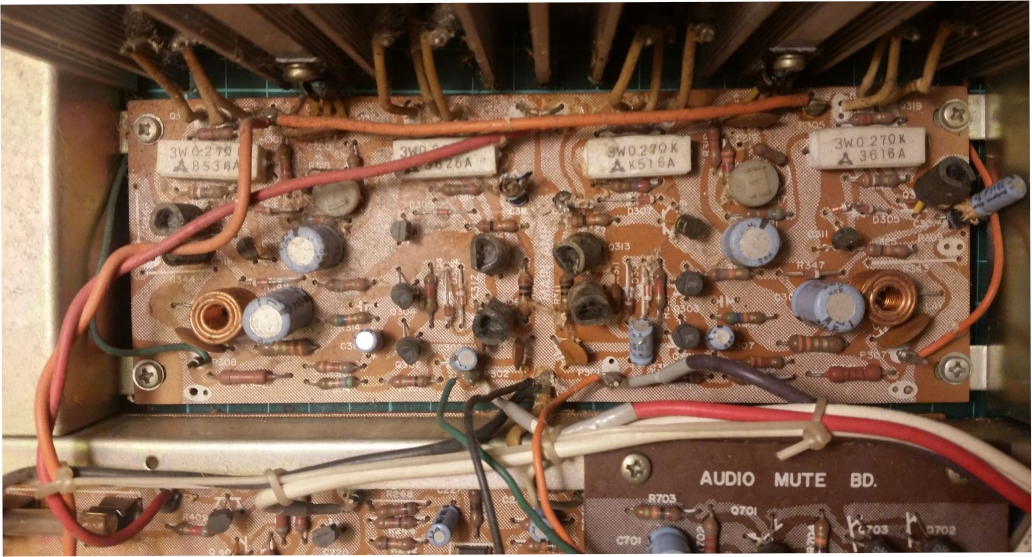
The board is labeled as "Main Amp" on the back side, just in case there were any questions about it.
Testing the main transistors
The amplifier is a transistor amplifier, which in this case means there are 4 main transistors that do all the heavy lifting. You won't need a schematic to find these: They are huge and attached to a big aluminium heatsink.
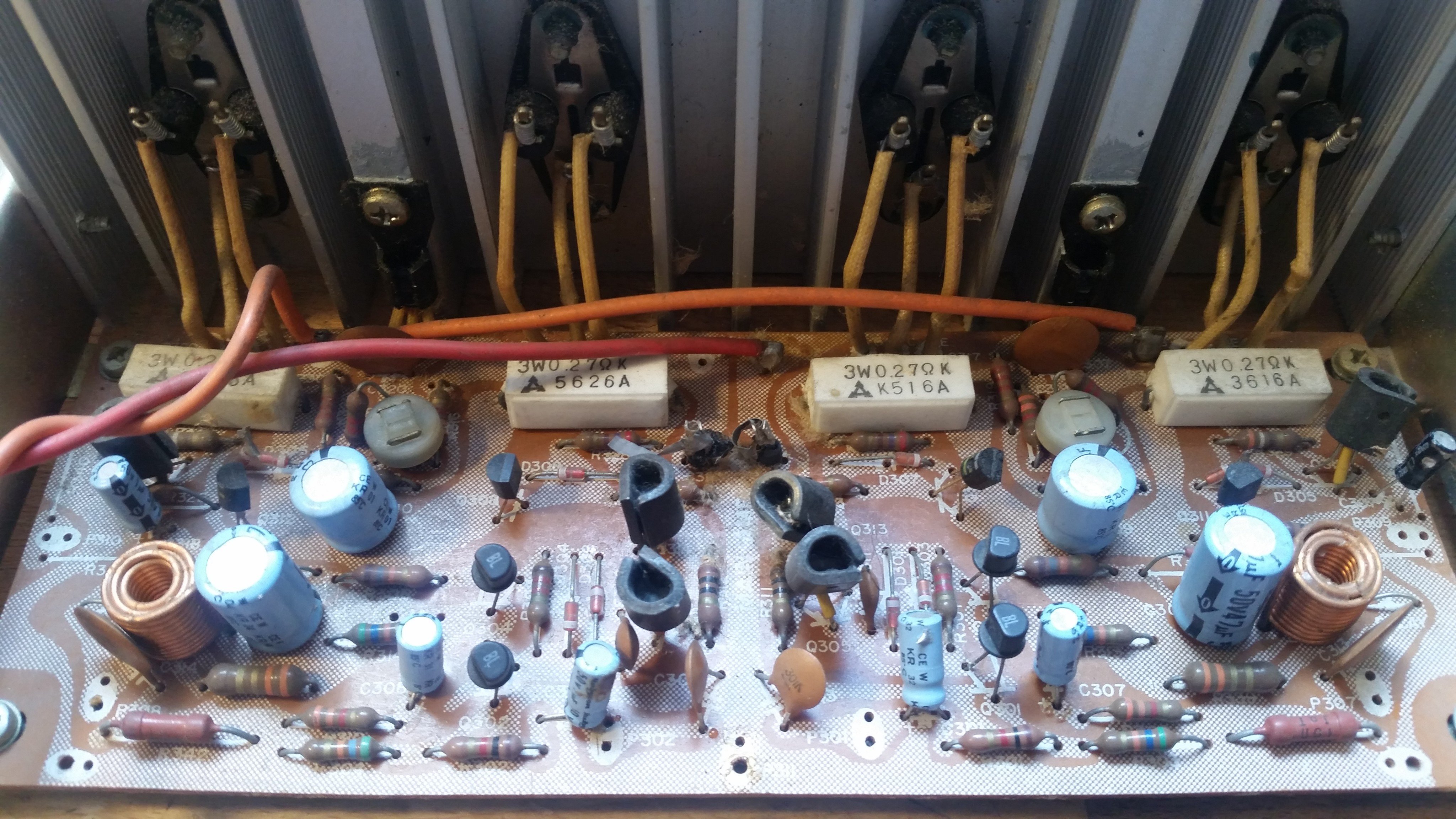
Even though the most common failiure in these kind of old devices are the capacitors which dry out, I want to make sure these are okay before doing anything else.
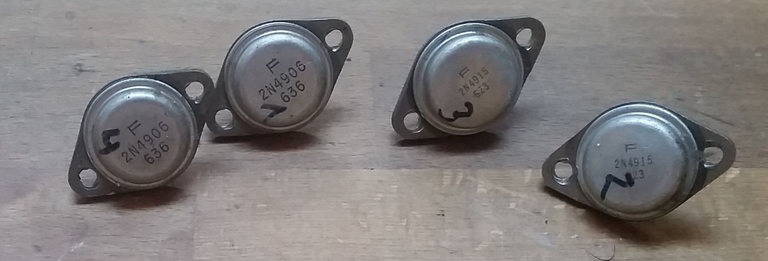
With a multimeter in "Diode Mode" I measured each of the four transistors form Collector to Emitter and from Collector to Base in both directions with these results:
| Transistor | 1 | 2 | 3 | 4 |
|---|---|---|---|---|
| C to E | 0.003V / 0.003V | OL / OL | 0.52V / OL | 0.57V / OL |
| C to B | 0.004V / 0.004V | 0.004V / 0.004V | 0.52V / OL | 0.57V / OL |
Without having looked up the datasheet for the particular transistors (2x 2N4915 and 2x 2N4906) I can already tell number 2 and probably number 1 are toast.
Trasistors have (when working) properties of a diode, meaning current can flow in one direction but not in the other, which is why I measure each pair of pins in both directions.
As you can see from the table above, 3 and 4 show "OL" (overload) for one direction while showing some reasonable value for the other. 1 and 2 on the other hand don't care anymore in what direction you try to push electrons through them. Guess they have seen better days.
Numbering components
The silk-screen of the PCB in question has numbering for the components on it, that should have mached the schematic. But they don't. Either it's the schematic for a different model or a different production year where they decided to change everything up. Additionally, quite a few of the markings are not readable anymore, which makes it hard to write down results and organize work.
I took a halfway decent picture of the pcb and used GIMP to write down labels for all componenets. I took all the ones I could read from the silk screen and defined new ones for the ones where I couldn't. Since I don't have a matching schematic anyway it doesn't really matter what the components are called, as long as the names are unique.
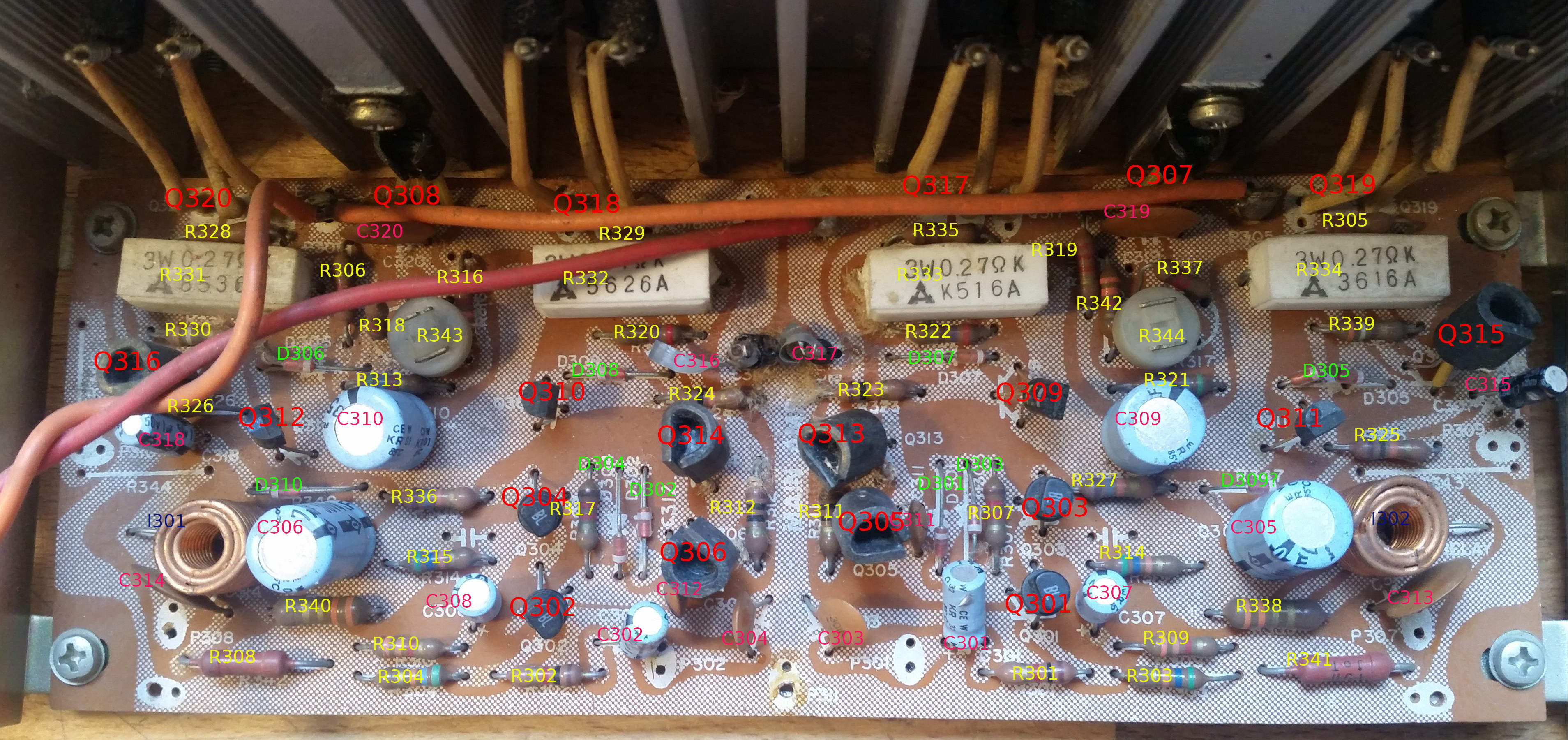
I will use the labels established above for everything from here on unless specified otherwise explicitely. They will also be used further along to create a full bill of materials.
Input power
Power comes from two wires to this board, positive and negative in respect to ground.
- Orange wire: -45V
- Red wire: +45V
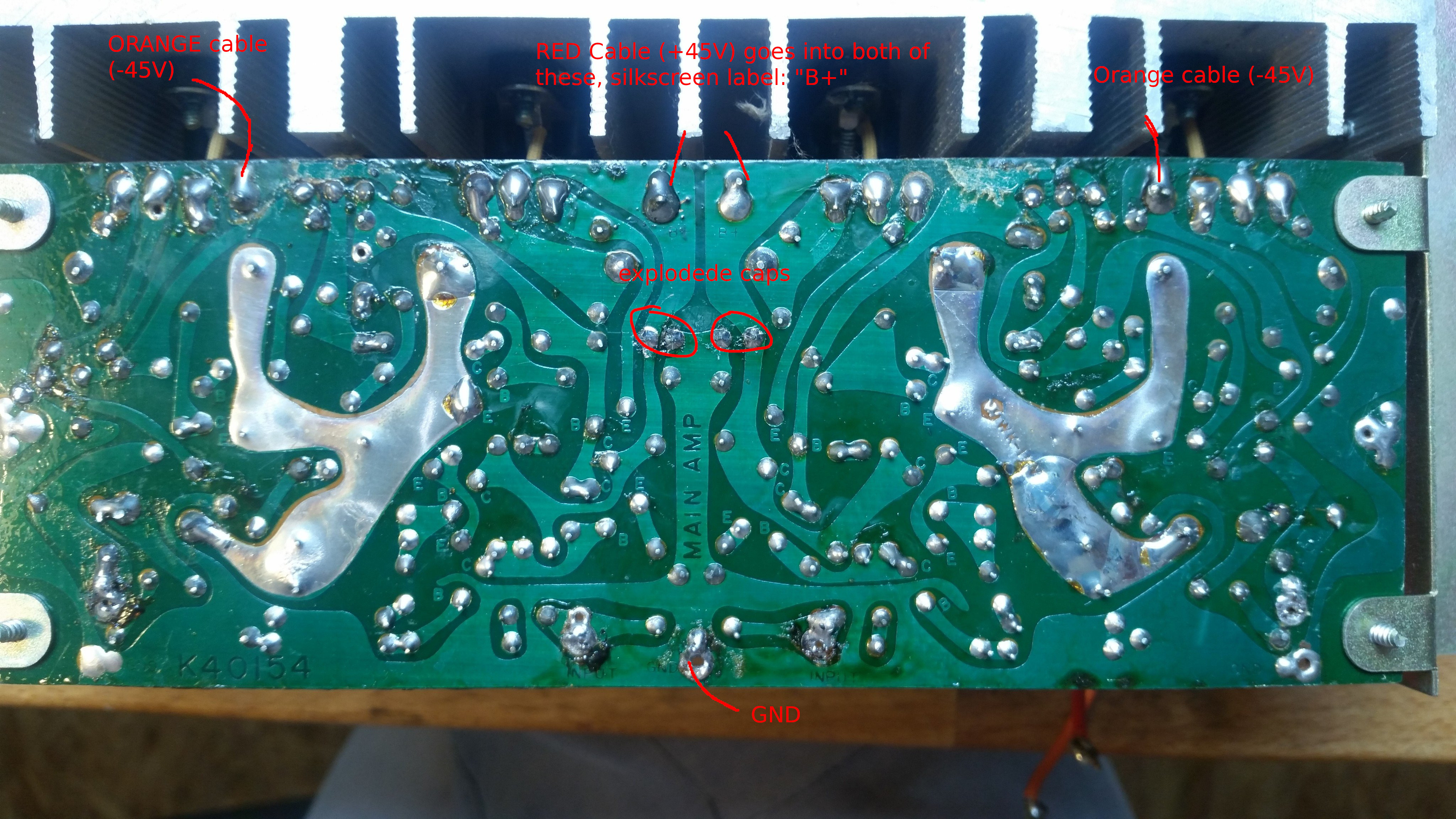
After replacing the blown fuse and taking out the main amp board, I measured these to verify that they still provide the correct voltage. Thankfully these are fine and the voltage is spot-on.
I think we can safly narrow down the problem to the main amp board.
Testing exploded caps to power source resistance
As you might have heart in the video linked in the first part of this series,
two caps left earth's orbit upon powering the amp. According to our numbering
above these are C316 and C317. There is a third cap that was in bad shape due
to it's age which I replaced too, even though it didn't blow up (yet).
| Exploded Caps | C316 [Ohm] | C317 [Ohm] |
|---|---|---|
| Negative pin to red wire | 0.7 | 0.1 |
| Positive pin to orange wire | 10k | 1.5k |
| Positive pin to GND | 12k | 12k |
| Negative pin to GND | 0 | 0 |
From the fact they have zero resistance to ground, I suspect these two where filtering capacitors in the times before the magic smoke.
Testing all other transistors
Guess there is no way around testing all the other transistors aswell. I really didn't want to desolder all 16 of them to test them and did a test on the board itself. The results where all over the place and didn't make much sense. I'll have to desolder them all to get a decent reading after all.
At first sight, it's clear they are not all the same. Q302, Q304, Q303 and
Q301 are more rounded and labeled all as "C1000". Then there are the ones
wrapped with a metal heatsink that might be something completely different. The
heatsink is glued and folded onto them and will need to be replaced after taking
it off.
To test the transistors I used a little "transistor tester" I bought from china as a kit some time ago.
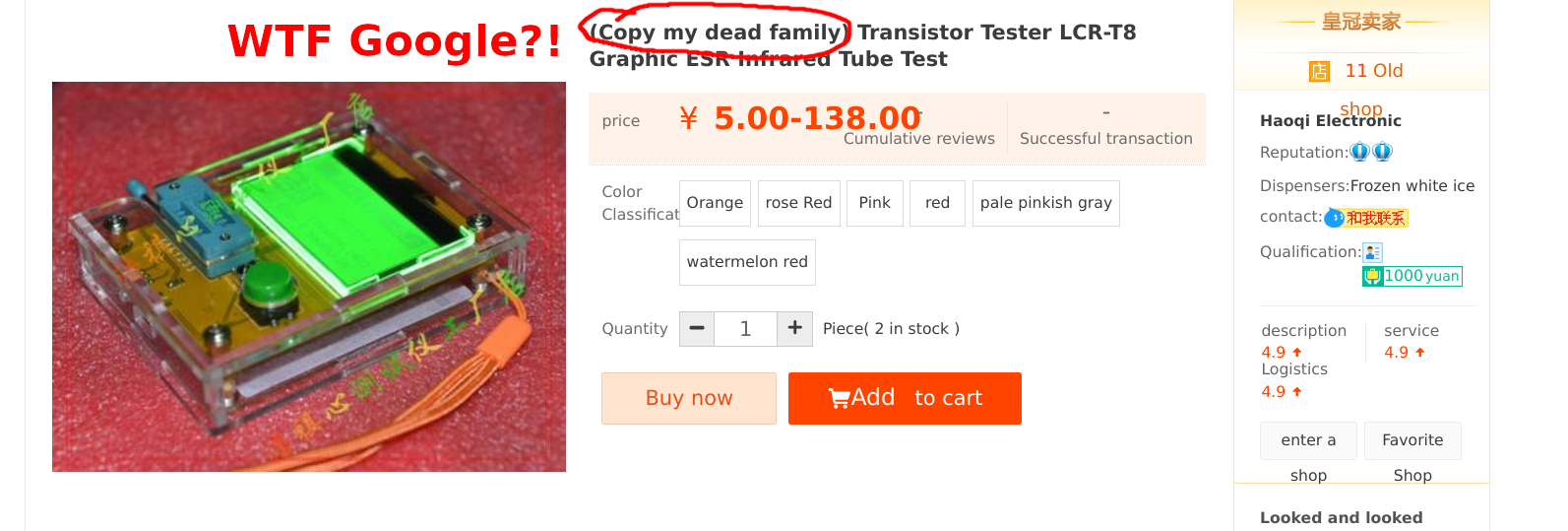
Apart from the pretty hilarious google translation, it's kind of handy even though I'm sure it's not the most accurate thing in the world. But it should give me a baseline to tell if a component is broken.
I desoldered all transistors and put them in a sorting box with neatly organized labels.
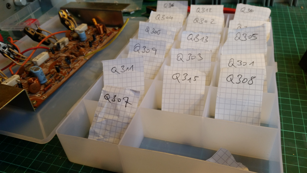
After that I put them all one by one in the tester and wrote down the measured values for the ones that got detected. I also peeled away the metal heatsinks and - like expected - broke all of them off. Anyway, it seems about one of each kind is broken (damn you, right stereo channel!), so I might buy more of each and replace them all.
Enought talk about transistors, we want numbers! Well, here you go:
| Transistors | Type | hFE | Uf [mV] | Label |
|---|---|---|---|---|
| Q301 | NPN | 429 | 679 | Tx C1000 6I |
| Q302 | NPN | 509 | 664 | Tx C1000 6H |
| Q303 | NPN | 558 | 664 | Tx C1000 6I |
| Q304 | NPN | 430 | 674 | Tx C1000 6H |
| Q305 | PNP | OL | OL | FMPS A56 |
| Q306 | PNP | 178 | 654 | FMPS A56 |
| Q307 | NPN | (MK) 9630 | ||
| Q308 | NPN | 428 | 693 | (MK) 9630 |
| Q309 | NPN | (MK) 9630 | ||
| Q310 | NPN | 140 | 713 | (MK) 9630 |
| Q311 | PNP | 304 | 708 | (MK) 9680 |
| Q312 | PNP | 234 | 658 | (MK) 9680 |
| Q313 | NPN | OL | OL | FMPS A06 |
| Q314 | NPN | 56 | 634 | FMPS A06 |
| Q315 | PNP | OL | OL | FMPS A56 |
| Q316 | PNP | 112 | 655 | FMPS A56 |
From the above transitors Q305, Q309, Q313 and Q315 are broken and will
have to be replaced. I will try to replace them all and get a new heatsink for
the ones the had it aswell.
Testing the diodes
If you compare electricity running through a wire as a hose with water running throught it, diodes could be thought of as a one-way valve: Electrons (current) can flow in one direction, but not in the other. More specificly, current will flow in a working diode from the anode to the cathode - but not the other way around. Symptons of a broken diode are that it does... well, something else.
Most multimeters have a "Diode Mode", so testing is pretty easy. On thing to note is that you will need to unsolder at least one terminal from the pcb to test them, otherwise the other components might interfere.
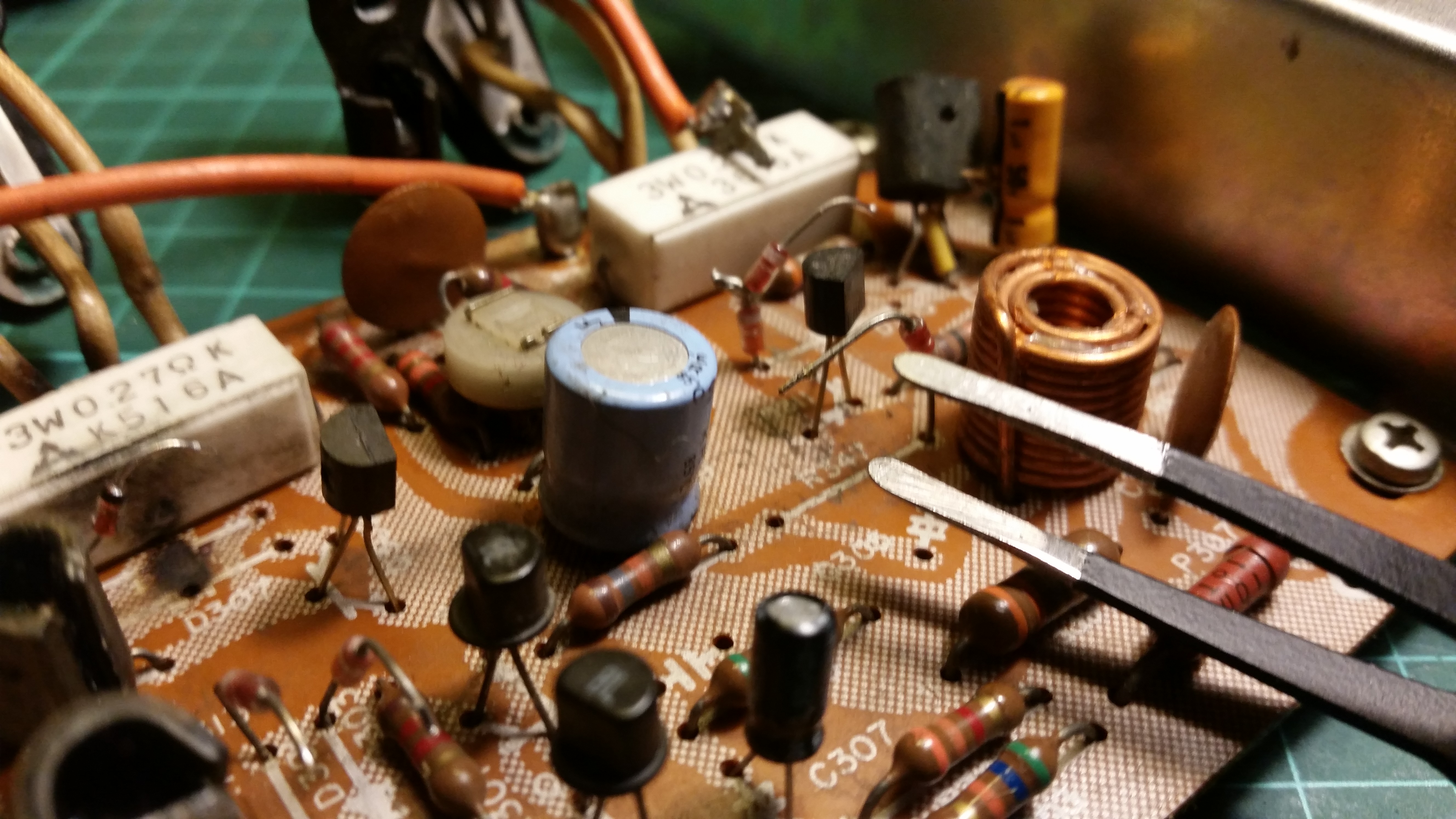
I unsoldered one leg of each diode and tested them all in both directions. Here are the results:
| Diodes | Anode to cathode | Cathode to anode |
|---|---|---|
| D301 | 0.6 | OL |
| D302 | 0.6 | OL |
| D303 | 0.6 | OL |
| D304 | 0.6 | OL |
| D305 (double) | 1.2 | OL |
| D306 (double) | 1.2 | OL |
| D307 | OL | OL |
| D308 | 0.6 | OL |
| D309 | 0.6 | OL |
| D310 | 0.6 | OL |
A reading of 0.6 and OL (overload) for a diode is pretty much spot on. Three things to notice here:
D307is broken as it doesn't conduct in any direction any more.- The values of
D305andD306are exactly double the value of the other ones. This is to be expected, as the pcb has actually two diodes soldered in series in these two spots for whavever reason. - All (working) diodes have the same values. Knowing this and seeing they all look the same from the outside, I'm pretty sure they are all the same model and can be changed between each other. One replacement type should fit all.
The clever internet tells me usual valus for silicon diodes are about 0.5V to 0.8V, so I guess these should be silicon diodes. Looking at pictures of silicon diodes further indicates they are.
Preliminary Conclusion
As an interim summary, what can be noted is that some of the transistors (main and other) are broken, as are some of the diodes. In a next step I'll have to figure out what I can replace them with, since the original parts will probably be not in production anymore.
I will replace all transistors, diodes and caps on this board since I expect that the unit price will be a few cents and the hardest part is to find out what I can use.
The innocent looking tables of results above took me quite a lot of hours to compile, but I feel the organisation of work is much easier now and it will pay out in the long run. All numbers are compiled in a glorious spreadsheet in case you want to see more details.
I have also taken a lot of pictures of all components from multiple sides. With more and more parts desoldered from the board I get a little paranoid, that I might not know how to put it back together later on. They will not all make it into this blog, let me know if you want a link to the complete album for some reason or any other information.
Also, part 3 is on the way, I'm too stubborn to stop now.